|
||||||||
| | Members RSVP | Home | | ||||||||
| DATE : | May 2nd, 2012 @ 4:30-6:00PM | ABSTRACT: | The semiconductor industry is facing some major changes. The Moore's Law that the Industry has undergone for the last 40 years is getting to some insurmountable barriers. One possibility to continue the race is the new concept "more than Moore" that put some of the effort into the back end-Packaging, namely 3D packaging and TSV (Through Silicon Vias). We will cover this new exciting technology, the problems, the issues and the future possibilities. For more information, please refer to an article HERE. |
|||||
| VENUE : | Nixon Peabody -2 Palo Alto Square 3000 El Camino | |||||||
PROGRAM : |
|
|||||||
| SPEAKER BIOGRAPHY | ||||||||
|
||||||||
| | Members RSVP | | ||||||||
| Sponsors |
||||||||
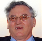 Dr. Beinglass has over 25 years of diversified experience in the semiconductor and semiconductor equipment industries in a variety of executive roles. He is currently an independent consultant to several semiconductor and semiconductor and LED equipment companies and is also the CTO of NuPGA and an angel investor working with several companies in the areas of new technologies,strategy, marketing and new applications. Before joining Applied Materials,Dr. Beinglass worked at Intel Corporation and IMP at a various positions, including process development manager and engineering manager of fab operations. While working at Intel he was the co-inventor of the Selective Tungsten Deposition. Dr.Beinglass has a Ph.D degree from Hebrew University of Jerusalem in materials science and holds 32 US patents.